
Introduction
In the quest for smaller, more powerful electronic devices, High-Density Interconnect (HDI) PCBs have become an essential component of modern circuit design. These printed circuit boards allow for the integration of complex circuitry within a compact space, enabling the creation of devices like smartphones, tablets, wearables, and more. As technology advances, HDI PCBs are at the heart of this evolution, providing the foundation for compact electronic designs.
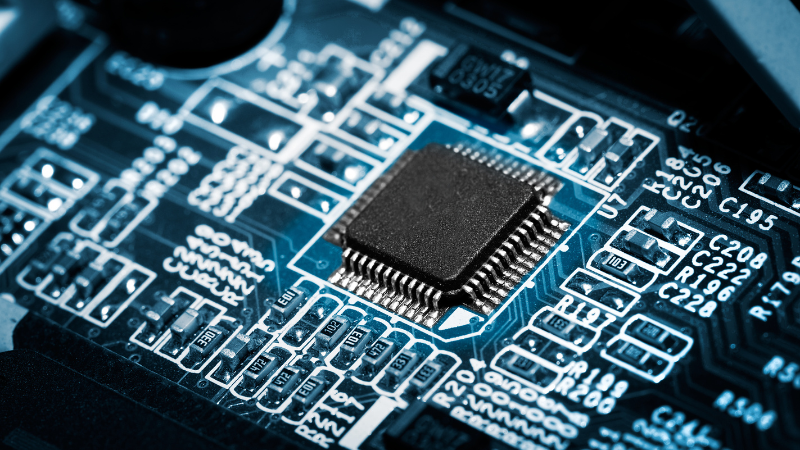
Characteristics of High-Density PCBs
High-Density PCBs are characterized by finer trace widths, smaller vias, and higher layer counts compared to traditional PCBs. These features allow for greater routing density, meaning more connections can be made within the same or smaller footprint. This is critical in today’s electronics, where space is often a limited resource.
Innovations in HDI PCB Design
One key innovation in HDI PCB design is the use of blind and buried vias. Traditional PCBs rely on through-hole vias that connect all the layers of a PCB. In contrast, blind vias connect an outer layer to one or more inner layers without passing through the entire board, while buried vias connect internal layers without reaching the surface. These techniques free up space on the surface layers for additional components and routing, significantly increasing the board’s density.
Another hallmark of high-density PCBs is the use of microvias—tiny vias that are typically less than 150 microns in diameter. Microvias are crucial in HDI design as they allow for finer routing and layer interconnects, essential for achieving miniaturization required in modern electronics. By reducing the size and increasing the number of vias, designers can pack more functionality into a smaller area.
Multi-Layer PCBs
Multi-layer PCBs are often a feature of HDI designs, with some boards incorporating 10 or more layers to manage the complexity of modern circuits. These layers allow for intricate signal routing, improved signal integrity, and enhanced performance, all while maintaining a small form factor. The use of multiple layers is important in high-speed and high-frequency applications, where maintaining signal quality is critical.
Benefits of High-Density PCBs
The benefits of high-density PCBs extend beyond saving space. They also contribute to improved electrical performance by reducing the distance that signals need to travel, which can lower resistance and inductance, leading to faster and more reliable circuits.
Challenges in Design and Manufacturing
Despite their advantages, designing and manufacturing high-density PCBs comes with challenges. The finer features and tighter tolerances require advanced manufacturing processes and precise control. The increased complexity also demands careful design considerations to avoid issues like crosstalk, signal degradation, and thermal hotspots. As a result, working with HDI PCBs often requires collaboration with specialized manufacturers who have the expertise and equipment to produce these intricate boards.
Additional Costs:
- Material Costs:
- High-Quality Substrates: HDPCBs often require advanced materials such as polyimide, Rogers, or other high-frequency substrates. These materials are more expensive than standard FR4 due to their superior electrical and thermal properties.
- Copper Thickness and Finish: HDPCBs use thinner layers of copper, which can require specialized processes to achieve the necessary copper weight without sacrificing performance, adding to the cost.
- Advanced Manufacturing Processes:
- Blind/Buried Vias: High-density PCBs often use blind and buried vias to connect different layers without increasing board thickness. The drilling and plating processes for these types of vias are more intricate and expensive than standard through-hole vias.
- Microvias: Microvias are used extensively in HDPCBs to connect layers in high-density designs. Creating microvias requires laser drilling technology, which increases costs compared to traditional mechanical drilling.
- Higher Layer Counts:
- Multi-layer Stacking: HDPCBs often have many layers (8 or more) to accommodate the complex routing and functionality needed for high-performance applications. The more layers a PCB has, the higher the manufacturing costs due to the extra materials, lamination, and drilling required.
- Increased Design and Testing Costs:
- Tighter Design Tolerances: The traces and spaces in HDPCBs are much smaller (typically below 100 µm), and the finer tolerances increase the likelihood of defects. Therefore, more time and resources are spent in design validation, DFM (Design for Manufacturability), and DFT (Design for Test) analysis.
- Increased Testing Complexity: With higher densities, in-circuit testing (ICT) and flying probe testing become more complicated and time-consuming, further increasing costs.
Manufacturing Challenges:
- Precision in Trace Width and Spacing:
- As HDPCBs require extremely fine trace widths and spacing, maintaining precision throughout the etching process is critical. Small variations can lead to signal integrity issues and potential shorts or opens, making the fabrication process more delicate and increasing the risk of yield loss.
- Impedance Control:
- High-speed HDPCBs must maintain precise impedance control to ensure signal integrity. This requires highly accurate layer stacking, trace width control, and dielectric constant management during fabrication, making it a more specialized process than standard PCB manufacturing.
- Thermal Management:
- Due to the high density of components and smaller traces, HDPCBs often face thermal management issues. The smaller form factor reduces the available surface area for heat dissipation, which may require advanced thermal materials or solutions like thermal vias or integrated heat sinks, complicating the design and manufacturing process.
- Lamination Challenges:
- HDPCBs with multiple layers and blind/buried vias undergo sequential lamination processes. Managing the integrity of these laminations without introducing defects such as delamination or misalignment is more complex than in traditional PCBs.
- Yield Issues:
- The precision and complexity of HDPCB manufacturing increase the risk of production defects. This leads to lower yields, driving up the cost per unit. Manufacturers often need to implement stringent quality control processes, including automated optical inspection (AOI) and X-ray inspection.
Conclusion
High-Density PCBs are a cornerstone of modern electronic design, enabling the creation of smaller, more powerful, and more efficient devices. As the demand for compact electronics continues to grow, the role of HDI PCBs will only become more critical. By pushing the limits of what is possible in circuit design, these PCBs are helping to shape the future of technology, driving innovation in everything from consumer electronics to industrial applications.