
Introduction to Multi-Layer PCBs
In the rapidly advancing world of electronics, where the demand for smaller, more powerful devices is ever-increasing, Multi-Layer PCBs have emerged as a crucial technology. These printed circuit boards, which feature multiple layers of conductive traces stacked on top of each other, allow for more complex and efficient circuit designs within a compact form factor. As devices become more sophisticated, the need for multi-layer PCBs grows, making them indispensable in modern electronic design.
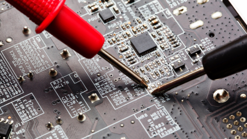
Structure and Composition
A multi-layer PCB consists of at least four conductive layers—two outer layers and one or more inner layers—sandwiched together with insulating material in between. The layers are interconnected through vias, which are tiny holes drilled through the board. By stacking multiple layers, designers can achieve intricate routing and signal management that would be impossible with single or double-layer PCBs.
Advantages of Multi-Layer PCBs
Increased Circuit Density
One of the primary advantages of multi-layer PCBs is the increased circuit density they offer. By adding more layers, designers can fit more circuits into a smaller space, making the overall device more compact. This is particularly important in applications like smartphones, tablets, and other portable devices, where space is at a premium. Multi-layer PCBs enable these devices to house complex circuits without increasing their size, contributing to the sleek and lightweight designs that consumers demand.
Enhanced Signal Integrity
Another significant benefit of multi-layer PCBs is their ability to improve signal integrity. In high-speed and high-frequency applications, maintaining signal quality is critical. Multi-layer PCBs allow for better separation of signal layers, ground planes, and power planes, which helps minimize interference and crosstalk between signals. This leads to faster, more reliable performance, which is essential in modern electronics where speed and accuracy are paramount.
Improved Thermal Management
The use of multi-layer PCBs also enhances thermal management. As devices become more powerful, they generate more heat, which needs to be efficiently dissipated to prevent overheating and ensure reliability. Multi-layer PCBs can incorporate dedicated heat dissipation layers or paths, allowing for better thermal distribution and management. This is especially important in high-power applications like power supplies, automotive electronics, and industrial equipment.
Reduced Electromagnetic Interference (EMI)
Additionally, multi-layer PCBs contribute to reduced electromagnetic interference (EMI). By strategically placing ground planes and shielding layers within the stack, designers can effectively control EMI, which is crucial for maintaining the performance and safety of electronic devices. This makes multi-layer PCBs particularly useful in environments where electronic noise could be an issue, such as in medical devices, communication systems, and aerospace applications.
Design and Manufacturing Challenges
Despite the numerous advantages, designing and manufacturing multi-layer PCBs comes with its own set of challenges. The increased complexity requires meticulous planning and design to ensure that all layers function together seamlessly. The manufacturing process is also more intricate, requiring precise control to align and bond the layers correctly. Any misalignment or defect in one layer can affect the entire board, leading to potential failures. Therefore, working with experienced manufacturers who specialize in multi-layer PCB production is crucial to achieving reliable results.
Conclusion: The Future of Multi-Layer PCBs
In conclusion, Multi-Layer PCBs are a cornerstone of modern electronic design, offering the ability to stack layers for greater efficiency, improved signal integrity, better thermal management, and reduced EMI. As electronic devices continue to evolve and demand more compact, powerful, and efficient solutions, multi-layer PCBs will remain a vital technology. By enabling more sophisticated and reliable circuit designs, these advanced PCBs are helping to drive innovation across various industries, from consumer electronics to aerospace, paving the way for the next generation of electronic devices.